Vedi pdf 
L298
.OPERATING SUPPLY VOLTAGE UP TO 46 V .TOTAL DC CURRENT UP TO 4 A .LOW SATURATION VOLTAGE .
.OVERTEMPERATURE PROTECTION .LOGICAL "0" INPUT VOLTAGE UP TO 1.5 V
(HIGH NOISE IMMUNITY)
DESCRIPTION
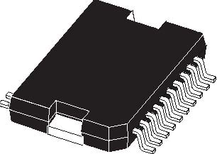
The L298 is an integrated monolithic circuit in a 15lead Multiwatt and PowerSO20 packages. It is a high voltage, high current dual full-bridge driver designed to accept standard TTL logic levels and drive inductive loads such as relays, solenoids, DC and stepping motors. Two enable inputs are provided to enable or disable the device independently of the input signals. The emitters of the lower transistors of each bridge are connected together and the corresponding external terminal can be used for the con-nection of an external sensing resistor. An additional supply input is provided so that the logic works at a lower voltage.
BLOCK DIAGRAM
DUAL FULL-BRIDGE DRIVER
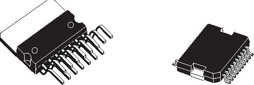
Multiwatt15 PowerSO20
ORDERING NUMBERS : L298N (Multiwatt Vert.) L298HN (Multiwatt Horiz.) L298P (PowerSO20)

ABSOLUTE MAXIMUM RATINGS
| Symbol | Parameter | Value | Unit |
|---|---|---|---|
| VS | Power Supply | 50 | V |
| VSS | Logic Supply Voltage | 7 | V |
| VI,Ven | Input and Enable Voltage | –0.3 to 7 | V |
| IO | Peak Output Current (each Channel) – Non Repetitive (t = 100µs) –Repetitive (80% on –20% off; ton = 10ms) –DC Operation | 3 2.5 2 | A A A |
| Vsens | Sensing Voltage | –1 to 2.3 | V |
| Ptot | Total Power Dissipation (Tcase = 75°C) | 25 | W |
| Top | Junction Operating Temperature | –25 to 130 | °C |
| Tstg, Tj | Storage and Junction Temperature | –40 to 150 | °C |
PIN CONNECTIONS (top view)

THERMAL DATA
| Symbol | Parameter | PowerSO20 | Multiwatt15 | Unit | |
|---|---|---|---|---|---|
| Rth j-case | Thermal Resistance Junction-case | Max. | – | 3 | °C/W |
| Rth j-amb | Thermal Resistance Junction-ambient | Max. | 13 (*) | 35 | °C/W |
(*) Mounted on aluminum substrate
PIN FUNCTIONS (refer to the block diagram)
| MW.15 | PowerSO | Name | Function |
|---|---|---|---|
| 1;15 | 2;19 | Sense A; Sense B | Between this pin and ground is connected the sense resistor to control the current of the load. |
| 2;3 | 4;5 | Out 1; Out 2 | Outputs of the Bridge A; the current that flows through the load connected between these two pins is monitored at pin 1. |
| 4 | 6 | VS | Supply Voltage for the Power Output Stages. A non-inductive 100nF capacitor must be connected between this pin and ground. |
| 5;7 | 7;9 | Input 1; Input 2 | TTL Compatible Inputs of the Bridge A. |
| 6;11 | 8;14 | Enable A; Enable B | TTL Compatible Enable Input: the L state disables the bridge A (enable A) and/or the bridge B (enable B). |
| 8 | 1,10,11,20 | GND | Ground. |
| 9 | 12 | VSS | Supply Voltage for the Logic Blocks. A100nF capacitor must be connected between this pin and ground. |
| 10; 12 | 13;15 | Input 3; Input 4 | TTL Compatible Inputs of the Bridge B. |
| 13; 14 | 16;17 | Out 3; Out 4 | Outputs of the Bridge B. The current that flows through the load connected between these two pins is monitored at pin 15. |
| – | 3;18 | N.C. | Not Connected |
ELECTRICAL CHARACTERISTICS (VS = 42V; VSS = 5V, Tj = 25°C; unless otherwise specified)
| Symbol | Parameter | Test Conditions | Min. | Typ. | Max. | Unit |
|---|---|---|---|---|---|---|
| VS | Supply Voltage (pin 4) | Operative Condition | VIH +2.5 | 46 | V | |
| VSS | Logic Supply Voltage (pin 9) | 4.5 | 5 | 7 | V | |
| IS | Quiescent Supply Current (pin 4) | Ven = H; IL = 0 Vi = L | 13 | 22 | mA | |
| Vi = H | 50 | 70 | mA | |||
| Ven = L Vi = X | 4 | mA | ||||
| ISS | Quiescent Current from VSS (pin 9) | Ven = H; IL = 0 Vi = L | 24 | 36 | mA | |
| Vi = H | 7 | 12 | mA | |||
| Ven = L Vi = X | 6 | mA | ||||
| ViL | Input Low Voltage (pins 5, 7, 10, 12) | –0.3 | 1.5 | V | ||
| ViH | Input High Voltage (pins 5, 7, 10, 12) | 2.3 | VSS | V | ||
| IiL | Low Voltage Input Current (pins 5, 7, 10, 12) | Vi = L | –10 | µA | ||
| IiH | High Voltage Input Current (pins 5, 7, 10, 12) | Vi = H ≤ VSS –0.6V | 30 | 100 | µA | |
| Ven = L | Enable Low Voltage (pins 6, 11) | –0.3 | 1.5 | V | ||
| Ven = H | Enable High Voltage (pins 6, 11) | 2.3 | VSS | V | ||
| Ien = L | Low Voltage Enable Current (pins 6, 11) | Ven = L | –10 | µA | ||
| Ien = H | High Voltage Enable Current (pins 6, 11) | Ven = H ≤ VSS –0.6V | 30 | 100 | µA | |
| VCEsat (H) | Source Saturation Voltage | IL = 1A | 0.95 | 1.35 | 1.7 | V |
| IL = 2A | 2 | 2.7 | V | |||
| VCEsat (L) | Sink Saturation Voltage | IL = 1A (5) | 0.85 | 1.2 | 1.6 | V |
| IL = 2A (5) | 1.7 | 2.3 | V | |||
| VCEsat | Total Drop | IL = 1A (5) | 1.80 | 3.2 | V | |
| IL = 2A (5) | 4.9 | V | ||||
| Vsens | Sensing Voltage (pins 1, 15) | –1 (1) | 2 | V |
ELECTRICAL CHARACTERISTICS (continued)
| Symbol | Parameter | Test Conditions | Min. | Typ. | Max. | Unit |
|---|---|---|---|---|---|---|
| T1 (Vi) | Source Current Turn-off Delay | 0.5 Vi to 0.9 IL (2); (4) | 1.5 | µs | ||
| T2 (Vi) | Source Current Fall Time | 0.9 IL to 0.1 IL (2); (4) | 0.2 | µs | ||
| T3 (Vi) | Source Current Turn-on Delay | 0.5 Vi to 0.1 IL (2); (4) | 2 | µs | ||
| T4 (Vi) | Source Current Rise Time | 0.1 IL to 0.9 IL (2); (4) | 0.7 | µs | ||
| T5 (Vi) | Sink Current Turn-off Delay | 0.5 Vi to 0.9 IL (3); (4) | 0.7 | µs | ||
| T6 (Vi) | Sink Current Fall Time | 0.9 IL to 0.1 IL (3); (4) | 0.25 | µs | ||
| T7 (Vi) | Sink Current Turn-on Delay | 0.5 Vi to 0.9 IL (3); (4) | 1.6 | µs | ||
| T8 (Vi) | Sink Current Rise Time | 0.1 IL to 0.9 IL (3); (4) | 0.2 | µs | ||
| fc (Vi) | Commutation Frequency | IL = 2A | 25 | 40 | KHz | |
| T1 (Ven) | Source Current Turn-off Delay | 0.5 Ven to 0.9 IL (2); (4) | 3 | µs | ||
| T2 (Ven) | Source Current Fall Time | 0.9 IL to 0.1 IL (2); (4) | 1 | µs | ||
| T3 (Ven) | Source Current Turn-on Delay | 0.5 Ven to 0.1 IL (2); (4) | 0.3 | µs | ||
| T4 (Ven) | Source Current Rise Time | 0.1 IL to 0.9 IL (2); (4) | 0.4 | µs | ||
| T5 (Ven) | Sink Current Turn-off Delay | 0.5 Ven to 0.9 IL (3); (4) | 2.2 | µs | ||
| T6 (Ven) | Sink Current Fall Time | 0.9 IL to 0.1 IL (3); (4) | 0.35 | µs | ||
| T7 (Ven) | Sink Current Turn-on Delay | 0.5 Ven to 0.9 IL (3); (4) | 0.25 | µs | ||
| T8 (Ven) | Sink Current Rise Time | 0.1 IL to 0.9 IL (3); (4) | 0.1 | µs |
1) 1)Sensing voltage can be –1 V for t ≤ 50 µsec; in steady state Vsens min ≥ – 0.5 V.
2) See fig. 2.
3) See fig. 4.
4) The load must be a pure resistor.
Figure 1 : Typical Saturation Voltage vs. OutputFigure 2 : Switching Times Test Circuits. Current.

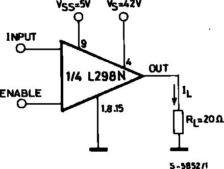
Note : For INPUT Switching, set EN = H For ENABLE Switching, set IN = H
Figure 3 : Source Current Delay Times vs. Input or Enable Switching.
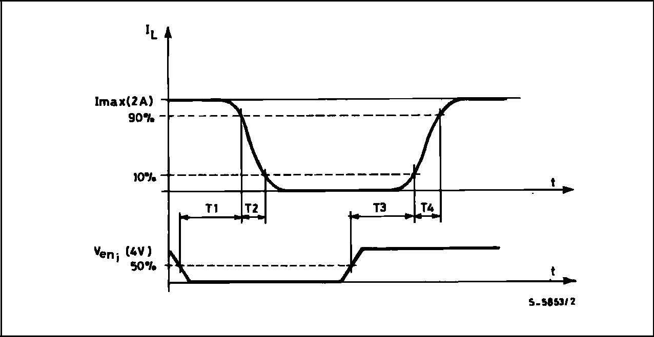
Figure 4 : Switching Times Test Circuits.
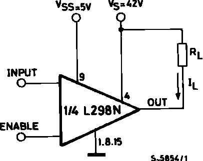
Note : For INPUT Switching, set EN = H For ENABLE Switching, set IN = L
Figure 5 : Sink Current Delay Times vs. Input 0 V Enable Switching.
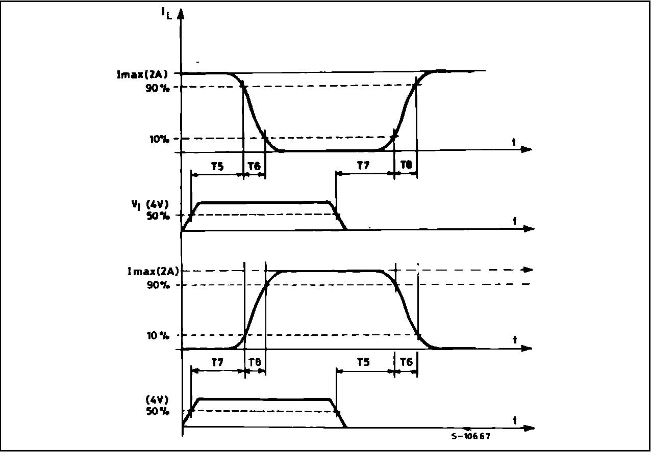
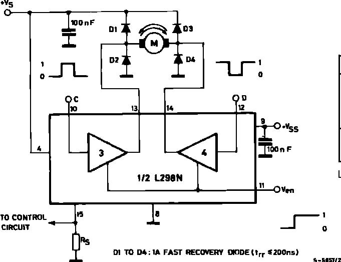
Figure 6 : Bidirectional DC Motor Control.
| Inputs | Function | |
|---|---|---|
| Ven = H | C = H ; D = L | Forward |
| C = L ; D = H | Reverse | |
| C = D | Fast Motor Stop | |
| Ven = L | C = X ; D = X | Free Running Motor Stop |
L = Low H = High X = Don’t care
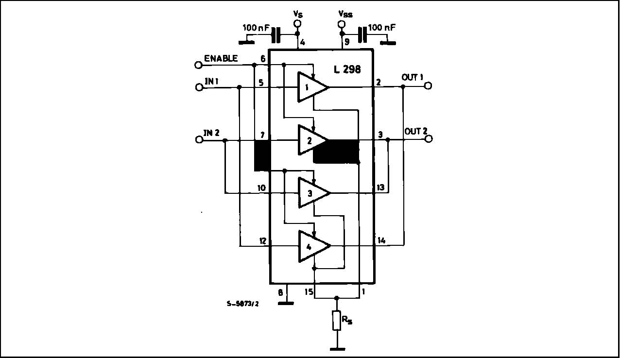
Figure 7 : For higher currents, outputs can be paralleled. Take care to parallel channel 1 with channel 4 and channel 2 with channel 3.
APPLICATION INFORMATION (Refer to the block diagram)
1.1. POWER OUTPUT STAGE The L298 integrates two power output stages(A; B). The power output stage is a bridge configuration and its outputs can drive an inductive load in common or differenzial mode, depending on the state of the inputs. The current that flows through the load comes out from the bridge at the sense output : an
external resistor (RSA ; RSB.) allows to detect the intensity of this current.
- INPUT STAGE
- Each bridge is driven by means of four gates the input of which are In1 ; In2 ; EnA and In3 ; In4 ; EnB. The In inputs set the bridge state when The En input is high ; a low state of the En input inhibits the bridge. All the inputs are TTL compatible.
- SUGGESTIONS
A non inductive capacitor, usually of 100 nF, must be foreseen between both Vs and Vss, to ground, as near as possible to GND pin. When the large capacitor of the power supply is too far from the IC, a second smaller one must be foreseen near the L298.
The sense resistor, not of a wire wound type, must be grounded near the negative pole of Vs that must be near the GND pin of the I.C.
Each input must be connected to the source of the driving signals by means of a very short path.
Turn-On and Turn-Off : Before to Turn-ON the Supply Voltage and before to Turn it OFF, the Enable input must be driven to the Low state.
3. APPLICATIONS Fig 6 shows a bidirectional DC motor control Schematic Diagram for which only one bridge is needed. The external bridge of diodes D1 to D4 is made by four fast recovery elements (trr ≤ 200 nsec) that
must be chosen of a VF as low as possible at the worst case of the load current. The sense output voltage can be used to control the
current amplitude by chopping the inputs, or to provide overcurrent protection by switching low the enable input.
The brake function (Fast motor stop) requires that the Absolute Maximum Rating of 2 Amps must never be overcome.
When the repetitive peak current needed from the load is higher than 2 Amps, a paralleled configuration can be chosen (See Fig.7).
An external bridge of diodes are required when inductive loads are driven and when the inputs of the IC are chopped ; Shottky diodes would be preferred.
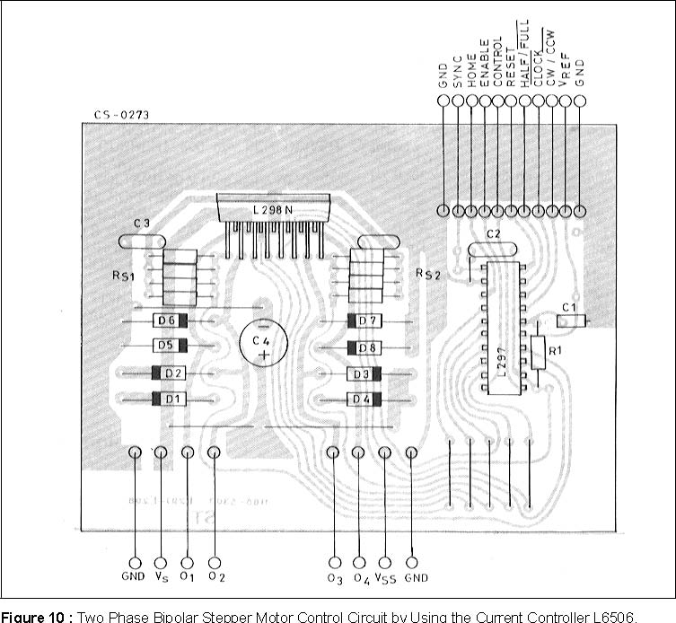
| This solution can drive until 3 Amps In DC operation | Fig 10 shows a second two phase bipolar stepper |
| and until 3.5 Amps of a repetitive peak current. | motor control circuit where the current is controlled |
| On Fig 8 it is shown the driving of a two phase bipolar | by the I.C. L6506. |
| stepper motor ; the needed signals to drive the in | |
| puts of the L298 are generated, in this example, | |
| from the IC L297. | |
| Fig 9 shows an example of P.C.B. designed for the | |
| application of Fig 8. | |
| Figure 8 : Two Phase Bipolar Stepper Motor Circuit. |
This circuit drives bipolar stepper motors with winding currents up to 2 A. The diodes are fast 2 A types.
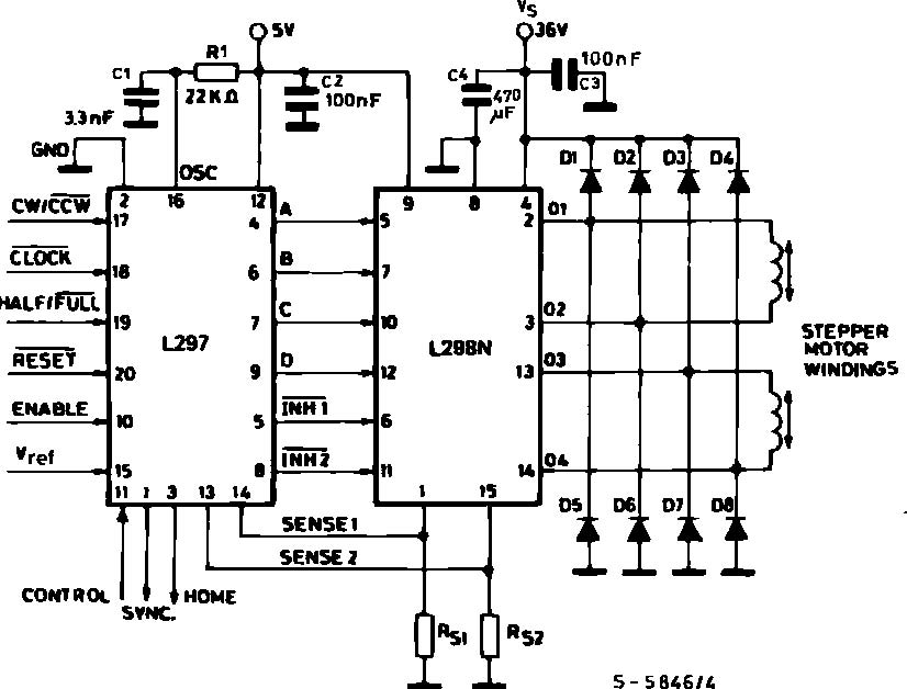
RS1 = RS2 = 0.5 Ω
VF ≤ 1.2 V @ I = 2 A D1 to D8 = 2 A Fast diodes { trr ≤ 200 ns
Figure 9 : Suggested Printed Circuit Board Layout for the Circuit of fig. 8 (1:1 scale).
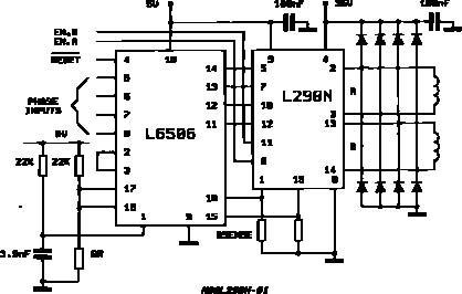
RR and Rsense depend from the load current
| DIM. | mm | inch | ||||
|---|---|---|---|---|---|---|
| MIN. | TYP. | MAX. | MIN. | TYP. | MAX. | |
| A | 5 | 0.197 | ||||
| B | 2.65 | 0.104 | ||||
| C | 1.6 | 0.063 | ||||
| D | 1 | 0.039 | ||||
| E | 0.49 | 0.55 | 0.019 | 0.022 | ||
| F | 0.66 | 0.75 | 0.026 | 0.030 | ||
| G | 1.02 | 1.27 | 1.52 | 0.040 | 0.050 | 0.060 |
| G1 | 17.53 | 17.78 | 18.03 | 0.690 | 0.700 | 0.710 |
| H1 | 19.6 | 0.772 | ||||
| H2 | 20.2 | 0.795 | ||||
| L | 21.9 | 22.2 | 22.5 | 0.862 | 0.874 | 0.886 |
| L1 | 21.7 | 22.1 | 22.5 | 0.854 | 0.870 | 0.886 |
| L2 | 17.65 | 18.1 | 0.695 | 0.713 | ||
| L3 | 17.25 | 17.5 | 17.75 | 0.679 | 0.689 | 0.699 |
| L4 | 10.3 | 10.7 | 10.9 | 0.406 | 0.421 | 0.429 |
| L7 | 2.65 | 2.9 | 0.104 | 0.114 | ||
| M | 4.25 | 4.55 | 4.85 | 0.167 | 0.179 | 0.191 |
| M1 | 4.63 | 5.08 | 5.53 | 0.182 | 0.200 | 0.218 |
| S | 1.9 | 2.6 | 0.075 | 0.102 | ||
| S1 | 1.9 | 2.6 | 0.075 | 0.102 | ||
| Dia1 | 3.65 | 3.85 | 0.144 | 0.152 |
OUTLINE AND
MECHANICAL DATA
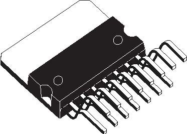
Multiwatt15 V

| DIM. | mm | inch | ||||
|---|---|---|---|---|---|---|
| MIN. | TYP. | MAX. | MIN. | TYP. | MAX. | |
| A | 5 | 0.197 | ||||
| B | 2.65 | 0.104 | ||||
| C | 1.6 | 0.063 | ||||
| E | 0.49 | 0.55 | 0.019 | 0.022 | ||
| F | 0.66 | 0.75 | 0.026 | 0.030 | ||
| G | 1.14 | 1.27 | 1.4 | 0.045 | 0.050 | 0.055 |
| G1 | 17.57 | 17.78 | 17.91 | 0.692 | 0.700 | 0.705 |
| H1 | 19.6 | 0.772 | ||||
| H2 | 20.2 | 0.795 | ||||
| L | 20.57 | 0.810 | ||||
| L1 | 18.03 | 0.710 | ||||
| L2 | 2.54 | 0.100 | ||||
| L3 | 17.25 | 17.5 | 17.75 | 0.679 | 0.689 | 0.699 |
| L4 | 10.3 | 10.7 | 10.9 | 0.406 | 0.421 | 0.429 |
| L5 | 5.28 | 0.208 | ||||
| L6 | 2.38 | 0.094 | ||||
| L7 | 2.65 | 2.9 | 0.104 | 0.114 | ||
| S | 1.9 | 2.6 | 0.075 | 0.102 | ||
| S1 | 1.9 | 2.6 | 0.075 | 0.102 | ||
| Dia1 | 3.65 | 3.85 | 0.144 | 0.152 |
OUTLINE AND
MECHANICAL DATA
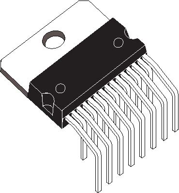
Multiwatt15 H

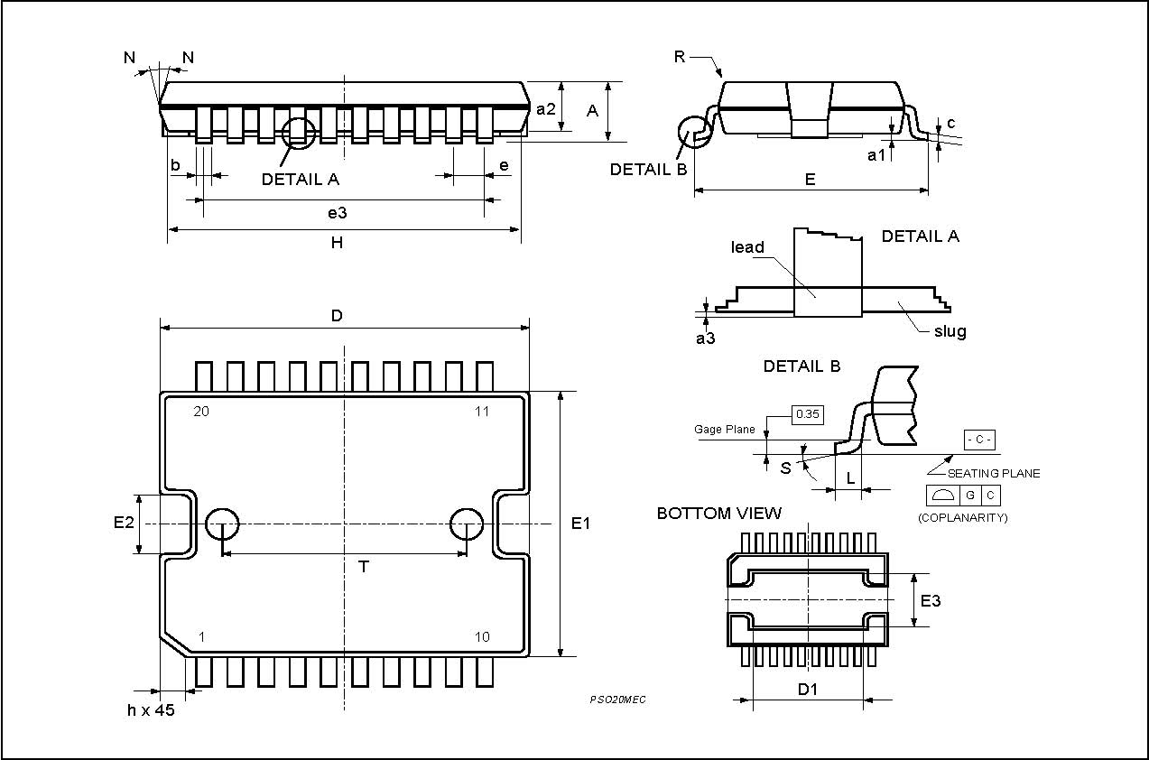
| DIM. | mm | inch | ||||
|---|---|---|---|---|---|---|
| MIN. | TYP. | MAX. | MIN. | TYP. | MAX. | |
| A | 3.6 | 0.142 | ||||
| a1 | 0.1 | 0.3 | 0.004 | 0.012 | ||
| a2 | 3.3 | 0.130 | ||||
| a3 | 0 | 0.1 | 0.000 | 0.004 | ||
| b | 0.4 | 0.53 | 0.016 | 0.021 | ||
| c | 0.23 | 0.32 | 0.009 | 0.013 | ||
| D (1) | 15.8 | 16 | 0.622 | 0.630 | ||
| D1 | 9.4 | 9.8 | 0.370 | 0.386 | ||
| E | 13.9 | 14.5 | 0.547 | 0.570 | ||
| e | 1.27 | 0.050 | ||||
| e3 | 11.43 | 0.450 | ||||
| E1 (1) | 10.9 | 11.1 | 0.429 | 0.437 | ||
| E2 | 2.9 | 0.114 | ||||
| E3 | 5.8 | 6.2 | 0.228 | 0.244 | ||
| G | 0 | 0.1 | 0.000 | 0.004 | ||
| H | 15.5 | 15.9 | 0.610 | 0.626 | ||
| h | 1.1 | 0.043 | ||||
| L | 0.8 | 1.1 | 0.031 | 0.043 | ||
| N | 10˚ (max.) | |||||
| S | 8˚ (max.) | |||||
| T | 10 | 0.394 | ||||
OUTLINE AND
MECHANICAL DATA
JEDEC MO-166
PowerSO20
(1) "D and F" do not include mold flash or protrusions. -Mold flash or protrusions shall not exceed 0.15 mm (0.006"). -Critical dimensions: "E", "G" and "a3"
L298
Information furnished is believed to be accurate and reliable. However, STMicroelectronics assumes no responsibility for the consequences of use of such information nor for any infringement of patents or other rights of third parties which may result from its use. No license is granted by implication or otherwise under any patent or patent rights of STMicroelectronics. Specification mentioned in this publication are subject to change without notice. This publication supersedes and replaces all information previously supplied. STMicroelectronics products are not authorized for use as critical components in life support devices or systems without express written approval of STMicroelectronics.
The ST logo is a registered trademark of STMicroelectronics
© 2000 STMicroelectronics – Printed in Italy – All Rights Reserved
STMicroelectronics GROUP OF COMPANIES
Australia - Brazil - China - Finland - France - Germany - Hong Kong - India - Italy - Japan - Malaysia - Malta - Morocco
Singapore - Spain - Sweden - Switzerland - United Kingdom - U.S.A.
http://www.st.com